10³ (10x10x10) LED Cube
This documents my progress in building a 10x10x10 LED Cube based on a Xilinx Spartan 3E XC3S500E FPGA and an Atxmega128 microcontroller.
Introduction
Work in in progress …. this page shows just a first glimpse :)
Prototyping was done on a Digilent Atlys board, after a proof of concept
has been implemented, as custom PCB with a XC3S500E has been designed.
Features
- 1000 High-Brightness Osram SMD LEDs
- 100 LEDs (one layer) are active simultaneously, layers are multiplexed on a 1:10 timebase
- Right now, PWM frequency is about 14MHz, multiplex frequency around 344 Hz
- With the USB interface (1MB/s) and direct video memory access a refresh-rate of about 250 Hz is possible
- Xilinx Spartan XC3S500E in PQ208 for low-level control and GPU implementation, most synthesized components running at 100 MHz
- ATxmega128A1 microcontroller for high-level control
- 7x TLC5941 high current (80mA) 12-bit PWM LED drivers
- 10x High-Side layer switches: MOSFET-driver + P-Channel MOSFET
- FT245 USB interface to a computer
- RN-42 Bluetooth UART interface to a computer
- LM75 temperature sensor
- MicroSD-Card slot
- SPI Flash onboard (for storing FPGA config)
- 3-axis accelerometer, gyroscope and magnetic field sensor
- Microphone amplifier with AGC (automatic gain control)
- Onboard 3.3V + 1.2V switching power supply
- 2.5V linear regulator
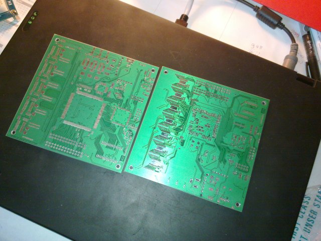
About the PCB
- Designed using Kicad (FOSS!)
- Exported as Gerber and Drill-Files
- Manufactured by MME PCB, 2 layers with 0.2mm structures.
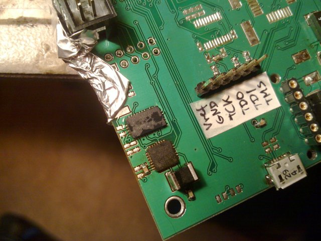
Configuring the FPGA
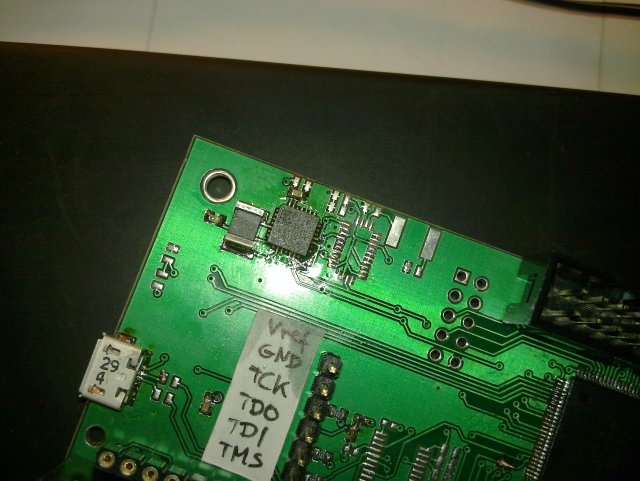
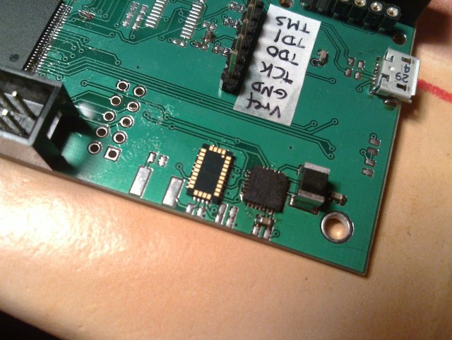
The FPGA can be configured directly via JTAG. However, during normal
operation it is configured via the Serial-Slave configuration mode by the
Atxmega. The configuration is stored on a SPI flash (AT45DB321) which is connected only to the microcontroller.
Memory-Mapped Interface to the FPGA
- FPGA's registers/LED-values are mapped into a virtual address space
- 16 bit address bus width
- 8 Bit data width
- Memory can be accessed by the Atxmega using its EBI and through USB using the FT245 USB protocol (see below)
- Direct access to the video RAM (VRAM) is possible by using addresses between 0 and 1000
- GPU's external registers can be accessed
- Further registers (e.g. for the UART synthesized on the FPGA) can be accessed
Interface between ATxmega and FPGA
- Virtual address space is connected ATxmega's address space by using the EBI bus in SRAM mode
- 8 Bit data width
- 16 bit address bus width (with address multiplexing)
- One chip select lines
- One read-enable, one write-enable line
- One interrupt line from FPGA to Atxmega
- WARNING: if you ever want to use EBI in SRAM CS ALE1 mode, keep in mind that the ALE1 signal is NOT driven on every access, but only if needed (the latch is assumed to be working all the time)
FT245 USB protocol
- Virtual address space can be accessed using a simple protocol via the FT245 USB interface
1 direction bit (read/write), 15 address bits, 8 data bits, each transfer
consists of 4 FIFO bytes
- 0 0 R/!W A14 A13 A12 A11 A10
- 0 1 A9 A8 A7 A6 A5 A4
- 1 0 A3 A2 A1 A0 D7 D6
- 1 1 D5 D4 D3 D2 D1 D0
A reply from the Cube consists just of the data bytes and is encoded as:
Graphics-Rendering on the FPGA
- The FPGA serves as a "graphics-card" for the microcontroller or a connected computer
- It offers rendering primitives which can be easily accessed through a couple of registers
- The following are implemented:
- Draw voxel (x1)
- Draw line (x1, x2) [using 3D-Bresenham in VHDL]
- Draw rectangle (x1, x2, x3) [executed on soft-processor]
- The following are planned:
- Draw circle (x1, r)
- Draw cube (x1, x2, x3, x4) [executed on soft-processor]
- The higher GPU functionality is implemented as a soft-core on the FPGA
- Idea: depending on the size of the GPU, more than a single one can be instantiated, so that several rendering operations can be done in parallel
External Register Documentation
- Coordinate-Registers
- X?_COORD_HIGH: x3 x2 x1 x0 y3 y2 y1 y0
- X?_COORD_LOW: z3 z2 z1 z0 * * * *
- Command-Register: GRAPHICS_CMD: c7 c6 c5 c4 c3 c2 c1 c0
- Command is executed on write on this register
- CMD_NOP = 0
- CMD_DRAW_VOXEL = 1
- CMD_DRAW_LINE = 2
- CMD_DRAW_RECT = 3
- Color-Registers
- DRAW_COLOR/FILL_COLOR: v7 v6 v5 v4 v3 v2 v1 v0
- Status-Register: * * * * * * * B
- B: busy indicator, if 1 the last command is not completed, yet
Programming the GPU
The higher GPU functions (except draw voxel and draw line) are executed
using a processor on the GPU. This section documents the instruction set
and the architecture of the processor.
- Harvard-architecture (separate program and data memories)
- Program memory is 4096 x 16 bit
- Data memory is 256 x 8 bit
- Instruction length is fixed to 16 bit, opcode is always 4 bit
- Register instruction: <opcode 3:0> <reg 3:0> <reg 3:0> <reg 3:0>
- Immediate instruction: <opcode 3:0> <reg 3:0> <immediate 7:0>
- Jump instruction: <opcode 3:0> <address 11:0>
- 16 scalar registers (8 bit wide)
- 16 vector registers (3x5 bit wide)
- SIMD (single instruction, multiple data) instructions on vector registers (currently addition and subtraction, moving data from/to scalar registers)
- No pipelining, yet
- Assembler written in Java, outputs program as ROM-file suitable to be loaded into the FPGA
Sensor Systems
TODO
Timing Diagrams
TODO
Hardware Details
High Side Switches
- Mosfet drivers: MCP 14E10-E/SN dual MOSFET driver, non-inverting
- P-FETs: IRF7416, 30V, 10A, 0.02 Ohm, 2.5W, small gate threshold voltage (about -1V) (and one SI 4435 BDY, they are interchangeable)
Power Supply
- Input to board: regulated 5V, with "enough" amps, directly powers MOSFET driver and P-FETs (and thus the LEDs), Bluetooth module and the following regulators
- LM2853-3.3 switching regulator: 3.3V, 3A - Vdd for most ICs
- LM2853-1.2 switching regulator: 1.2V, 3A - FPGA core voltage
- LM2937-2.5 linear regulator: 2.5V, 400mA - FPGA configuration voltage
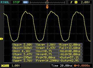
Eliminating Ghosting
Problem: If high-side layer switches are (almost) unloaded, they will take
a long time to completely switch off (due to capacitances at the drain
of the FET, I guess and in the wiring).
The situation looks like this:
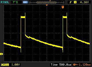
It can clearly be seen that the voltage does not reach 0V during one
multiplexing cycle. Thus some LEDs may be switched on very dim although they
should not.
The solution is to add a load-resistor of 1kOhm between the drain of each
high-side P-FET and ground. At 5V there will only be 5V/1kOhm = 5mA flowing
through each of these load resistors, but the effect is magnificient:
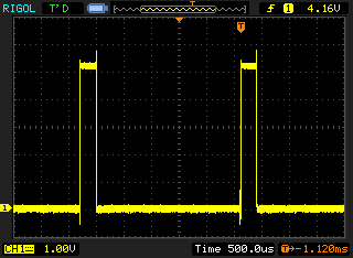
No more ghosting :-)
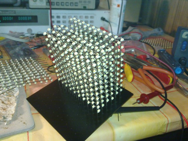
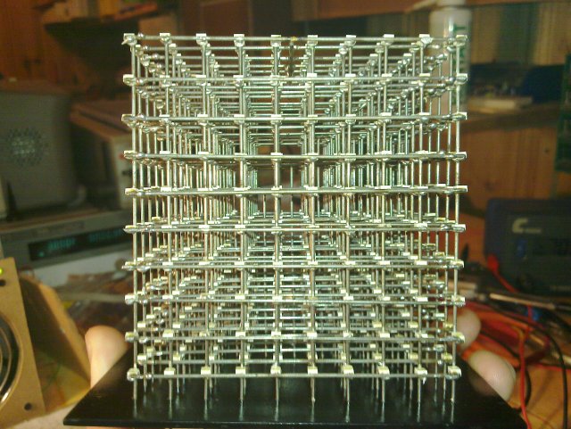
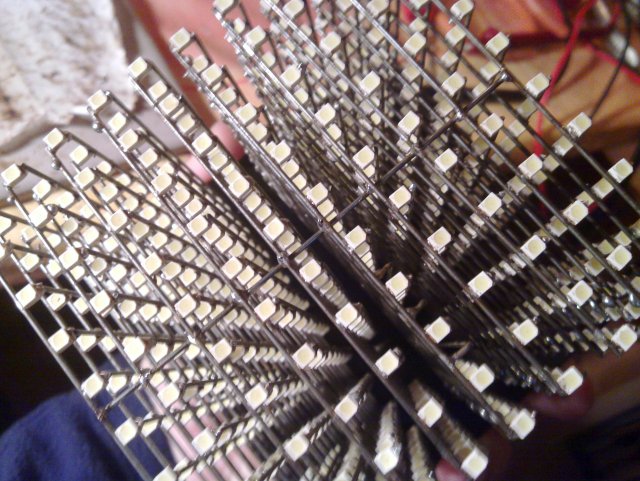
Pictures
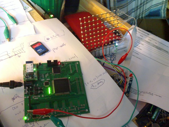
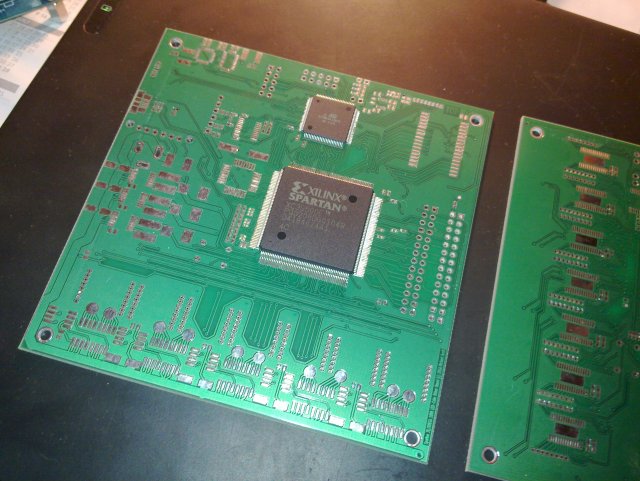
The PCB has arrived!
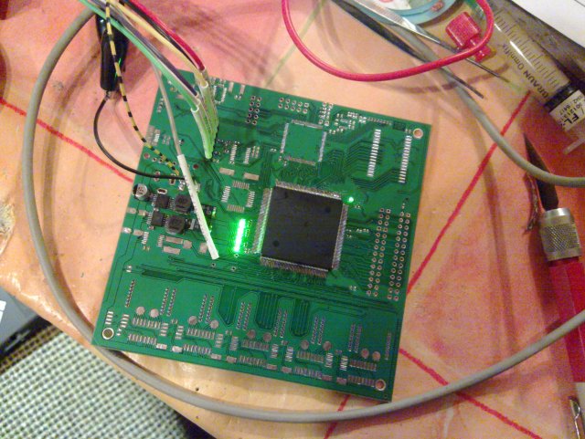
Configuring the FPGA for the first time with the Platform Cable … I have seldom been so happy about a couple of LEDs lighting up!
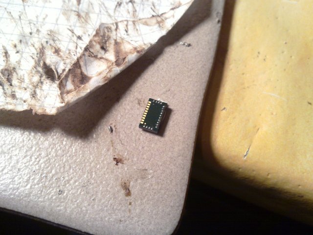
How to solder LGA parts:
First, make a BGA (Ball Grid Array) out of the LGA (Land Grid Array).
Use flux … LOTS of flux.
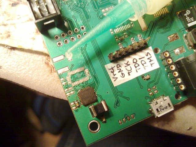
Heat it up using hot air and wait for the part to float by itself into
the correct position.
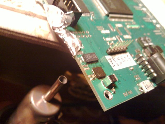
Clean up the flux-mess
The PWM-Clock, note that this is captured on an oscilloscope with only 20 MHz analog bandwidth, so the real waveforms might actually be more square :-)
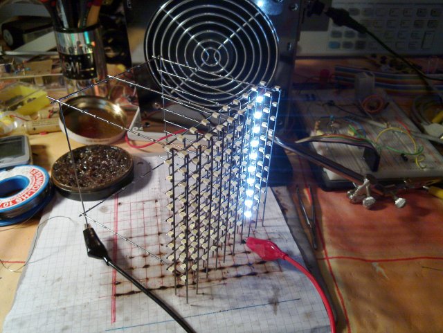
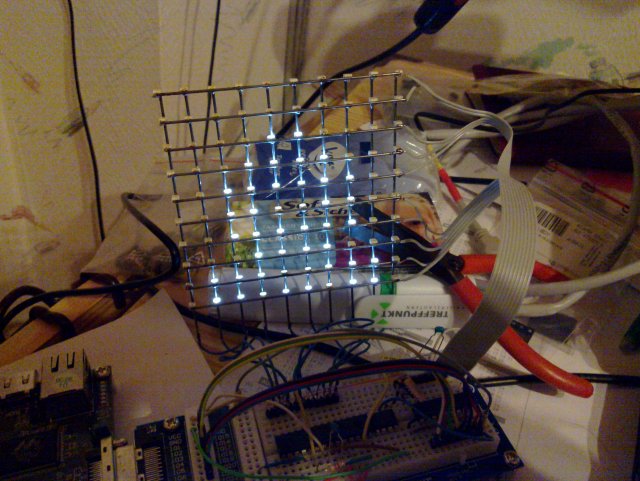
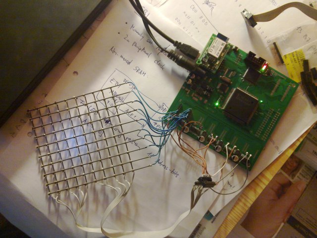
2D matrix connected to the PCB
Arranging the slices on the drilled and painted top piece.
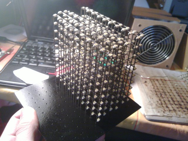
After fixing the slices.
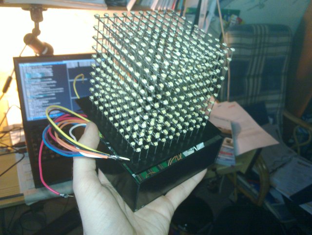
Demonstration of how it may finally look like :-)
Videos
http://www.facebook.com/v/2749925007562
Lessons Learned
Xilinx/ISE/XST:
- Always specify INPUT_JITTER for your input clock or insert a frequency that is slightly greater as the frequency printed on your crystal oscillator!
- PAR routes somewhere along the "bleeding edge" - in other words: just a little bit of (unspecified) Jitter on your clock input *WILL* break everything sooner or later!
- Always synchronize freaking external inputs! Not synchronizing them will make hell freeze over (your statemachines might end up in unreachable states and much more fun!)
- The allmighty XST does not (version 13.1) seem to be able to infer the range of integer datatypes in VHDL, you should always specify a range or you might end up with 32 bit registers holding values from 0 to 5 (or less)
- Most of the Xilinx Tools are bitches!
Atxmega:
- EBI in SRAM CS ALE1 mode: the ALE1 signal is NOT driven on *every* access, but only if needed (the latch is assumed to be perfectly working *all the time*)
LEDs/Drivers/MOSFETs:
- Always connect the LEDs with common anode, as low-side-drivers are much more common (and probably much cheaper, if you can find good integrated high-side-drivers at all)
|
